|
Jenoptik with High-Performance Products at SPIE Photonics West 2015
2/14/2015 |
|
|
At North America's leading photonics industry fair - the SPIE Photonics West - from February 10 to 12, 2015 in San Francisco, Jenoptik will be presenting product highlights of its Optical Systems and Lasers & Material Processing divisions. Furthermore, Jenoptik will again support young entrepreneurs in the SPIE Startup challenge.
At SPIE Photonics West 2015 the Optical Systems division of Jenoptik is presenting, amongst others, precision optics for the semiconductor industry and improved light modulators. The Lasers & Material Processing division puts highly efficient laser diodes and a powerful ultrashort pulse laser in the focus. In addition, Jenoptik will be showcasing the product ranges of both divisions at booth 1423 in the South Hall of the Moscone Center.
As in the past years, Jenoptik will again be the founding partner of the SPIE Startup Challenge, a competition of the international society for optics and photonics (SPIE). At this event, young entrepreneurs from the field of optical technologies will present their business ideas and products to an expert jury.
Products at a glance: Optical Systems division
New Precision Optics for the Semiconductor Equipment Industry
With its new modular concept, Jenoptik's Optical Systems division is one of the few suppliers of the next generation of high-performance optical systems.
The Optical Systems division sets out to develop an innovative modular solution, with the aim of overcoming the limitations of the drop-in assembly of high-performance optical systems, which has been the conventional option until now. As a result, an optical system was developed that uses a stack-mounting technology, which makes it possible to meet the increasing demanding requirements of the market. The patented stress-free mounting technology of the optical elements is one feature that guarantees the maximum level of accuracy. The mount, which was designed specifically for DUV optics with a high numerical aperture, holds optical components without the aid of adhesives.
This new concept means that individual elements and the optical system as a whole can be mounted precisely, quickly and above all robustly with maximum reproducibility. In order to compensate for aberrations within the optical system, the optics can be combined with manual or motorized compensating and adjustment elements. The stack-mounting, the recently developed compensating elements and the stress-free mounts together create a modular platform, which offers a high level of flexibility in terms of the system size as well as a low adaptation risk.
Jan Werschnik, an expert in precision optics at Jenoptik, is committed to this new technology: "A number of customers have already tried out the concept, which has surpassed the targets set for it. We have put a lot of time into proving the high level of accuracy of these precision optics systems. We now talk about stability in terms of nanometers and are able to provide quantitative proof of this. The modified fixing method also provides the required permanent alignment of the optics in relation to one another."
One of the main business activities of Jenoptik's Optical Systems division is the development and production of customer-specific systems for the semiconductor equipment industry.
Over the past few years, requirements in terms of accurately measuring imaging quality and polarization properties have increased significantly within this market segment. With its new concept, Jenoptik is one of the few suppliers that are able to produce the next generation of high-performance optical systems.
More Compact Design of Light Modulators with USB Interface
Jenoptik's Optical Systems division will be presenting their new generation of SLM series (Spatial Light Modulator) liquid crystal modulators for the modulation of ultra-short laser pulses, which are making their trade show debut.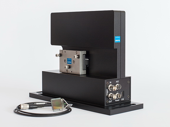
Thanks to the more compact design, this highly-specialized equipment for laser light modulation is more straightforward to integrate into different superstructures with existing computer technology and meets the customer's requirement of having an optical setup that is more compact.
Jenoptik's liquid crystal modulators can change the phase, amplitude and polarization of light in the wavelength range of 430 to 1600 nanometers and are inserted as variable masks in so-called pulse shapers, in other words, optical setups for the modulation of ultra-short laser pulses.
The large liquid crystal mask, with individual 10 or 13 millimeter pixels, makes it possible to use high-power lasers. To minimize disruptive back reflections, Jenoptik can tailor anti-reflection coatings to the individual customer. The liquid crystal modulator works in transmission, but can however also be operated in a reflective mode with the optional mirror. The modulators are easy to control thanks to lab software such as LabView, MATLAB and C-Interface.
Typical areas of application include ultra-short-time spectroscopy and microscopy, micro material processing and coherent control of chemical and biochemical reactions.
Products at a glance: Lasers & Material Processing division
High-Performance Laser Diodes for a Wide Range of Applications
High-performance laser diodes have become established as compact, efficient and wear-free beam sources because many material processing applications require a high constant optical power output while maintaining a high electro-optical efficiency at the same time. High-performance laser diodes are also used in pulsed lasers with extremely high pulse energies whose pump source is a high-power QCW laser bar. At SPIE Photonics West 2015, the Lasers & Material Processing division of Jenoptik will present new products for both areas of application.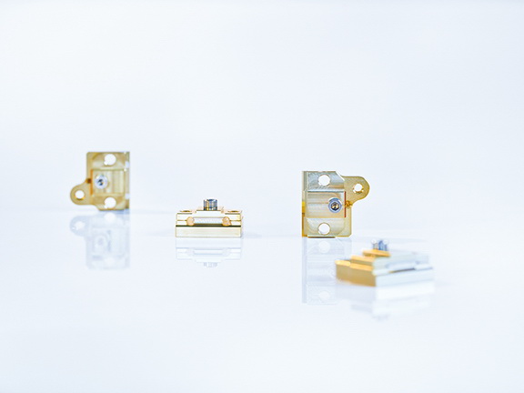
With the new laser bars emitting at 880 nanometers that are optimized for optical peak output powers, Jenoptik meets the pump source requirements of high-energy pulse lasers. The laser bars provide a reliable peak power of up to 500 Watts at an electro-optical efficiency (WPE) of more than 55 percent while having a beam divergence of 11 degrees in the slow axis direction and 45 degrees in the fast axis direction.
Jenoptik also offers a new class of laser bars for use in material processing applications. They have a continuous output power of 200 Watts and an emission wavelength of 940 nanometers and are mounted on a passive CN heat sink. This patented heat sink provides highly efficient heat removal through cooling of the laser bar on both sides.
Powerful and Reliable Femtosecond Laser
Since 2009, the Lasers & Material Processing division of Jenoptik has successfully developed femtosecond lasers for industrial material processing. Based on reliable diode-pumped disk laser technology, the latest generation - the JenLas® femto 10 - provides customers with perfect beam quality, a power of 10 watts and pulse energies of up to 50 microjoules. In addition to that, this femtosecond laser is very flexible because it has an adjustable pulse repetition frequency, a fast beam switch for pulse picking and reduction of repetition rate and allows frequency doubling from 1,030 to 515 nanometers.
The JenLas® femto 10 is a reliable and versatile femtosecond laser for micro-materials processing in the Jenoptik portfolio, offering unparalleled processing quality while keeping heat influence minimal at the same time and a material ablation rate that is up to four times higher than that of picosecond lasers having the same power. Due to the high processing speeds and the fact that extensive rework is not necessary anymore, the JenLas® femto 10 allows for a significant increase in productivity. The improved femtosecond laser has been developed for industrial high-quality applications and 24/7 continuous operation. A special focus was put on easy system integration, high reliability and stability guaranteeing reproducible application results. Jenoptik supports customers by offering application tests in the in-house application laboratory and by providing service personnel world-wide.
The ultrashort pulses of 400 to 800 femtoseconds of the JenLas® femto 10 allow non-thermal ablation for almost all materials; that is the production of extremely small workpiece and surface structures without melting or deleterious thermal effects. Examples for cutting and drilling include very small medical implants such as stents made of nitinol, stainless steel or (bio-)polymers and various materials for automobile manufacturing and watchmaking. It is even possible to process hard and brittle materials such as diamonds and glass or composite materials (for example CFRP) and obtain excellent results using the JenLas® femto 10. Moreover, the laser is suitable for thin-layer ablation or structuring surfaces, e.g. in the semiconductor industry or in medical technology. |
|
Related Exhibition:
|
|
|
 |
|
SPIE Photonics West 2015
|
The Marketplace for the Photonics, BioPhotonics, and Laser Industry
2/7/2015 - 2/12/2015
Venue: The Moscone Center, San Francisco CA, United States
|
|
|
|
|
|
|